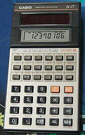
Solar-powered scientific calculator
Because solar cells are semiconductor devices, they share many of the same processing and manufacturing techniques as other semiconductor devices such as computer and memory chips. However, the stringent requirements for cleanliness and quality control of semiconductor fabrication are a little more relaxed for solar cells. Most large-scale commercial solar cell factories today make screen printed poly-crystalline silicon solar cells. Single crystalline wafers which are used in the semiconductor industry can be made into excellent high efficiency solar cells, but
they are generally considered to be too expensive for large-scale mass production.
Poly-crystalline silicon wafers are made by wire-sawing block-cast silicon ingots into very thin (180 to 350 micrometer) slices or wafers. The wafers are usually lightly p-type doped. To make a solar cell from the wafer, a surface diffusion of n-type dopants is performed on the front side of the wafer. This forms a p-n junction a few hundred nanometers below the surface.
Antireflection coatings, which increase the amount of light coupled into the solar cell, are typically next applied. Over the past decade, silicon nitride has gradually replaced titanium dioxide as the antireflection coating of choice because of its excellent surface passivation qualities (i.e., it prevents carrier recombination at the surface of the solar cell). It is typically applied in a layer several hundred nanometers thick using plasma-enhanced chemical vapor deposition (PECVD). Some solar cells have textured front surfaces that, like antireflection coatings, serve to increase the amount of light coupled into the cell. Such surfaces can usually only be formed on single-crystal silicon, though in recent years methods of forming them on multicrystalline silicon have been developed.
The wafer then has a full area metal contact made on the back surface, and a grid-like metal contact made up of fine "fingers" and larger "busbars" are screen-printed onto the front surface using a silver paste. The rear contact is also formed by screen-printing a metal paste, typically aluminium. Usually this contact covers the entire rear side of the cell, though in some cell designs it is printed in a grid pattern. The paste is then fired at several hundred degrees Celsius to form metal electrodes in ohmic contact with the silicon. Some companies use an additional electro-plating step to increase the cell efficiency. After the metal contacts are made, the solar cells are interconnected in series (and/or parallel) by flat wires or metal ribbons, and assembled into modules or "solar panels". Solar panels have a sheet of tempered glass on the front, and a polymer encapsulation on the back. Tempered glass cannot be used with amorphous silicon cells because of the high temperatures during the deposition process.
No comments:
Post a Comment